.png)

ZPrize 2023 1st place winner
Introduction
Zero-Knowledge Proofs (ZKPs) are extremely computationally expensive, with Multi-Scalar-Multiplication (MSM) being the dominant part in many ZK proof systems. The 2023 ZPrize competition (Prize 1A) challenged participants to accelerate MSMs on either NVIDIA GPUs or AMD FPGAs.
The work described in this blog post was a collaboration between ZPrize 2022 winner Niall Emmart of Yrrid Software and Ingonyama’s Tony Wu. Niall was the architect of the project and Tony was in charge of the implementation.
To achieve enhanced performance over a set of elliptic curves, the team implemented, for the first time on an accelerator platform, the batched affine method for elliptic curve addition. This approach significantly reduces the computational burden associated with MSMs, marking a significant advance in hardware-based ZK computation. Some key highlights of the design:
- Able to fit three EC-adders on the U250 FPGA — this is 1.5x better than state of the art
- Achieved the same performance on both the BLS12–381 and BLS12–377 curves
- Achieved >99% pipeline efficiency for most of the MSM computation
This blog post delves into the specifics of the implementation, with an overview of the architecture as well as a deep dive into some of the key components that make the design work. Finally we discuss the implications for future ZK hardware and what the next steps are towards our ultimate goal, end-to-end ZK acceleration.
ZPrize 2023
The challenge for this year’s competition (Prize 1A) involved computing a batch of four MSMs of size 2²⁴ as quickly as possible, using the AMD Alveo U250 FPGA card.
A significant change from last year’s competition is the requirement to support both the BLS12–381 and BLS12–377 curves. Previously, the competition focused solely on the BLS12–377 curve, used by Aleo. During last year’s competition, it was discovered that the BLS12–377 curve could be mapped to a more computationally efficient “Twisted Edwards” representation. The new requirement was intended to advance the state-of-the-art in MSM processing more broadly, as BLS12–381 lacks a Twisted Edwards representation.
Multi-Scalar-Multiplication
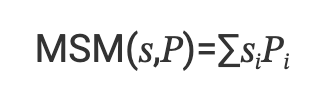
Multi-Scalar Multiplication (MSM) is a fundamental operation in elliptic curve cryptography (ECC). It involves computing the sum of the element-wise products of a vector of scalars 𝑠 and a vector of elliptic curve points 𝑃.
In the case for BLS12–381, the scalars are 255-bits wide and each coordinate of a point is 381-bits. This means that an MSM is extremely computationally intensive when the vector sizes are large (in our case 2²⁴).
The fastest algorithm for computing MSMs is the Bucket Method (aka Pippenger’s Algorithm), which decomposes the problem into smaller MSMs by slicing the scalars into 𝑚 windows of 𝑤 bits.
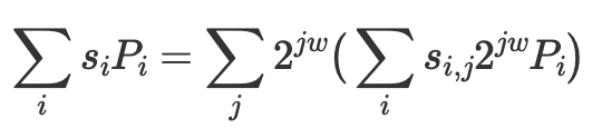
So we can compute 𝑚 small MSMs in parallel and then sum up the partial results.
We will not describe in more detail the bucket method in this blog as it is the typical way to compute MSMs. For more information see:
- Pippenger Algorithm for Multi-Scalar Multiplication (MSM)
- zkStudyClub: Multi-scalar multiplication: state of the art & new ideas with Gus Gutoski
Elliptic Curve Addition
Since scalar multiplication is defined as repeated addition of a point, the primary computational cost for an MSM is the huge number of elliptic curve additions required. Therefore it is important to optimize the amount of FPGA resources required to implement an EC-adder.
The formula in affine coordinates for an ec-addition 𝑃+𝑄=𝑅 is:
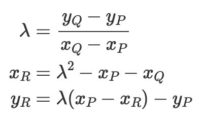
We can see that in order to compute 𝜆 we need to perform a division. Since we are operating on a prime field, this requires a modular inversion, which is extremely expensive.
Therefore most previous MSM designs opted to extend the typical (𝑥,𝑦) coordinates (called Affine Coordinates) into Extended Coordinates, which trades the division for significantly more multiplications. For example, using Extended Jacobian coordinates (𝑥,𝑦,𝑧𝑧)+(𝑥,𝑦):
Batched Affine EC-Addition
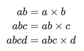
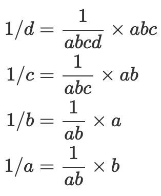
There is a well known method called the montgomery trick which can be used to compute the inverses for a batch of values cheaply. That is, if we wanted to compute 1/𝑎, 1/𝑏, 1/𝑐, and 1/𝑑, we could first batch the inputs by multiplying them together:
Then compute the batched inverse:
Then we can obtain the individual inverses by unbatching them:
While this seems simple in theory, it is difficult to implement. This is because this formulation does not consider the latency of the multipliers required to implement this efficiently, nor does it consider all the intermediate values that must be saved in order to unbatch.
In our design we implement batched affine EC-addition in the spirit of the Montgomery Trick, but with our own two-step batching method that makes it possible to physically implement on an FPGA.
Architecture Overview
For our design we chose to slice the scalars into 21 windows of 13-bits each. We use the signed slices trick in order to reduce the slices to only 12 physical bits.
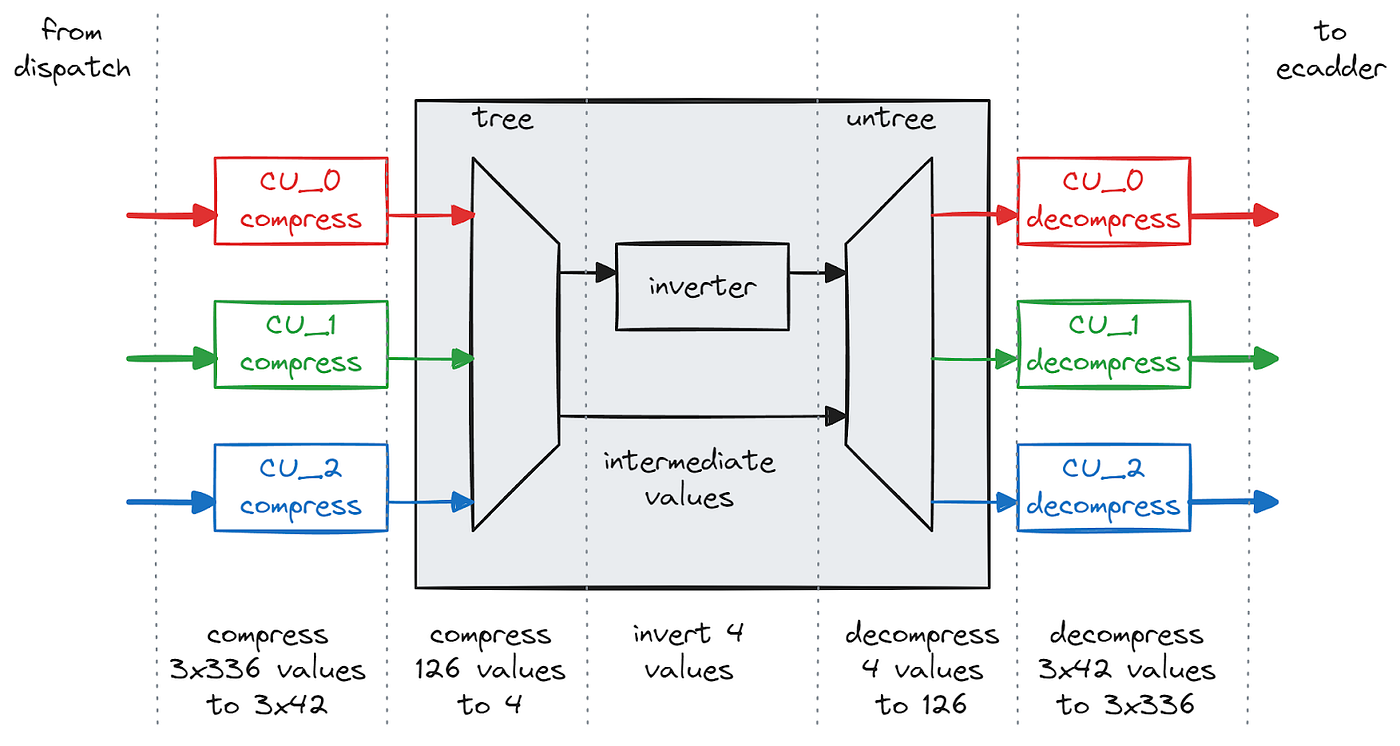
Our design consists of the following key components:
- A main ingress / egress unit, that reads the points and scalars from device memory and receives the start MSM command from the host.
- Three compute units (CUs) for EC-additions
* Each compute unit is responsible for 7 out of 21 windows and is capable of performing one EC-addition every clock cycle.
* Each compute unit contains 6 modular multipliers. - A shared inverter capable of computing 3 inverses every clock cycle.
* The inverter contains 2 modular multipliers.
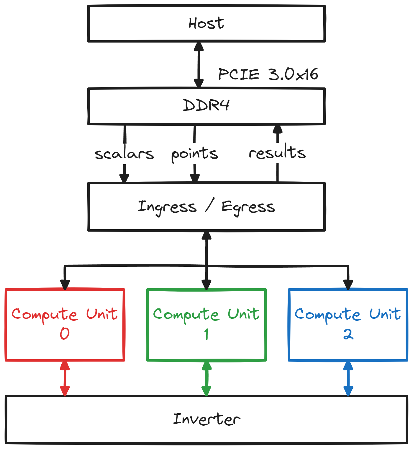
Now let’s have a look at the data flow:
Setup Phase
- The host programs the FPGA card with either our BLS12–381 or BLS12–377 design
- The host transfers the 2²⁴ points to the device memory (DDR4).
Compute Phase
NOTE: We will refer to magic numbers such as 42, 336, and 1008. These numbers were strategically chosen while considering the various parameters and constraints of our design, however we will not go into details in this blog.
- The host transfers the first set of scalars to device memory
* (Note we can overlap the next set of scalar transfers with the first execution) - The ingress unit reads pairs of scalars and points from memory and broadcasts them to three compute units.
- Each compute unit will batch together 336 EC-operations before sending the batch to the shared inverter.
- The inverter further aggregates the batches into a single batch of 1008 field elements.
- For every batch of 1008 the inverter only performs 4 actual inversions using a highly optimized Extended Euclidean Algorithm.
- The inverses are un-batched through a reverse process and sent back to the compute units.
- Finally the actual EC-additions are performed and the result is saved back into their respective window memories.
Finalization Phase
- Once all the points and scalars have been consumed, the contents of all the window memories are sent back to the host.
- The host computes the final sum and returns the result.
Compute Unit Design
Zooming in on the compute unit, we see that a point-scalar pair first flows through a Point Tagger, this tags the incoming point with a retrieval-ID and saves the point into a cache. The scalars then flow to a slicer, which converts the scalar into bucket indices and other metadata. These metadata packets are then sent to their respective window lanes.
Within each window lane, the meta-data packets first enter a collision handler which is designed to avoid bucket collisions. A collision happens when an EC-operation tries to access the same bucket as an earlier operation that is still in-flight (i.e. the result has not been written back yet). The collision handler attempts to avoid collisions by reordering operations as they come in from the slicer. Buckets are marked locked when they are in-flight and unlocked when they are written back. When an access to a locked bucket is detected, the collision handler attempts to swap the new operation with a previously pending operation that no longer collides (i.e. the bucket it addresses has been unlocked). The colliding operation is saved into a pending buffer, while the non-colliding operation is forwarded down the pipeline to the window memories. In our simulations we see that the number of operations in the pending buffer stabilizes at around 35 entries throughout the MSM computation (while assuming that an operation will be in-flight for ~3500 clock cycles).
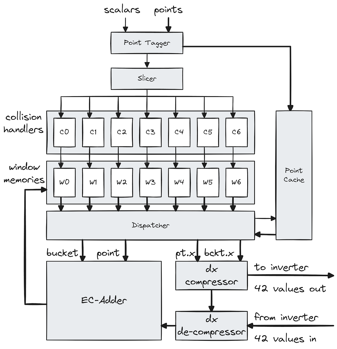
After indexing and retrieving their respective bucket values, the operations wait to be dispatched in round-robin order by the dispatcher. During dispatch, the retrieval-ID that was contained in the meta-data is used to retrieve the relevant point from the cache. This method of point caching is important as it saves us from having to keep a separate copy of the point with each EC-operation through the collision handlers and would result in 7x the memory usage. Once an ID/tag has been accessed seven times the cache entry is freed and the ID can be reused.
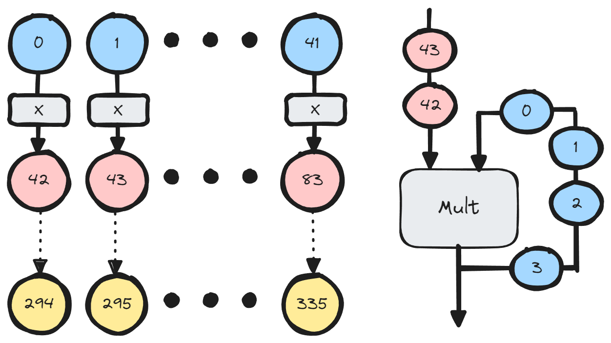
Once dispatched, the point (𝑃) and bucket (𝑄) are queued on the input of the EC-adder and their x-coordinates are fed to the dx compressor, which is the first stage in computing the batched inversion. We first compute the denominator, dx = xᵩ — xₚ. We then batch together 336 denominators (𝑑𝑥’s) and regard this data as 8 vectors of 42 elements each:
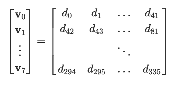
The dx compressor sequentially multiplies the 8 vectors element-wise to produce a single vector of length 42, computing:
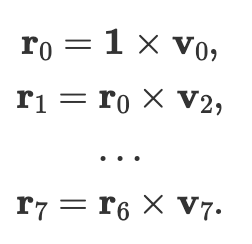
This is done by sequentially feeding the vector elements into a multiplier that recycles the result back as the second input operand. This is the first step in our batching/compression process and is done locally within each compute unit. The final 42 products are then sent to the shared inverter, while the intermediate products are saved for use during the unbatching/decompression process.
NOTE: This means that our multiplier must have less than 42 cycles of latency in order to be efficient (i.e. stall-free).
When the 42 inverses come back, they are decompressed back to 336 inverses, by using the intermediate products produced by the compressor. These inverses then allow the EC-adder to execute and write the results back into the window memories.
Inverter Design
Now zooming into the shared inverter, we see that it receives 42 field values from each of the three compute units and further compresses the 126 field elements to just 4 field elements using a tree-like structure.
The figure below shows a mini-example of how we would compress 8 field elements to 2 field elements. Below, we assume we have elements 𝑎,𝑏,𝑐,𝑑,𝑒,𝑓,𝑔,ℎ, and we treat these as the leaf nodes of two binary trees. The parents of the leaf nodes are computed by the products of the children, and this continues recursively up to the root nodes. In order to be able to decompress the batched inverses (1/𝑎𝑏𝑐𝑑, 1/𝑒𝑓𝑔ℎ), we need to save the values of all of the intermediate nodes.
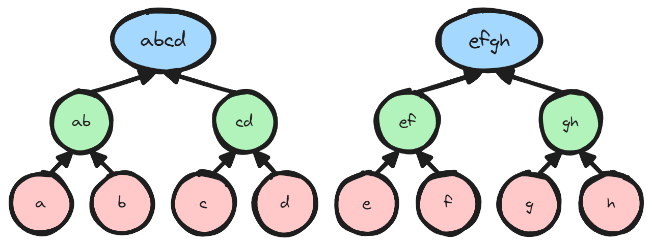
After inversion we start with the root nodes and work our way back to individual inverses. At each node, we can derive the left child by multiplying by the previously saved right child. Similarly we can derive the right child by multiplying by the previously saved left child.
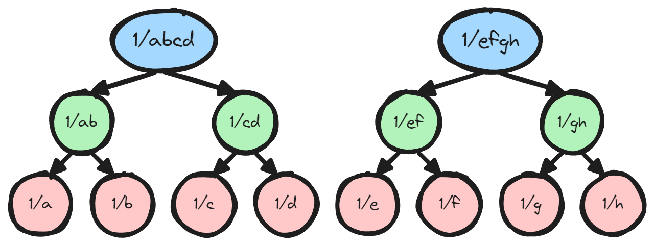
In the full case, we have 126 leaf nodes and 4 root nodes. The reason we chose to compress down to and invert 4 field elements instead of 1 is again due to the latency of our multipliers.
We use two fully pipelined multipliers inside the inverter, one for the compressor tree and one for the decompressor untree. By fully pipelined we mean that each multiplier can process one multiplication every cycle, however the results will not be available instantly. There is a certain latency in clock cycles between when an input is presented and when the corresponding output is ready. As we process our way up the layers of the tree, there are less and less parallel operations that we can use to fill up the pipeline. Therefore our processing efficiency drops as we approach the root, and we determined it would actually decrease our inverter throughput if we compressed all the way to one root.
Multipliers
Due to the low-latency requirements for some of our multipliers, we experimented with several multiplier designs. We came up with three multiplier designs which are optimized for different purposes:
- Low Latency Multiplier (LL)
* Latency: 22 cycles @ 250MHz — 38 cycles @ 400MHz
* DSPs: 413
* LUTs: ~24K - Medium Area Multiplier (MA)
* Latency: >42 cycles
* DSPs: 372
* LUTs: ~27K - Low Area Multiplier (LA)
* Latency: >80 cycles
* DSPs: 346
* LUTs: ~38K
In the end we only used the LL multipliers and the MA multipliers. We determined that while using LA multipliers would save us more DSPs, it created more routing congestion and would prolong compile time.
Results
We submitted both our BLS12–377 and BLS12–381 designs to ZPrize. Both designs were clocked at 250MHz, achieving 750M EC-operations per second. This allowed our design to compute a batch of four 2²⁴ MSMs in 2.04 seconds! This is significant especially for the BLS12–381 for which there does not exist a Twisted Edwards representation. This result is 2.5X faster than last year’s ZPrize winner (scaled to 2²⁴) which only supports BLS12–377.
The image below shows the physical mapping of our three compute units onto the FPGA.
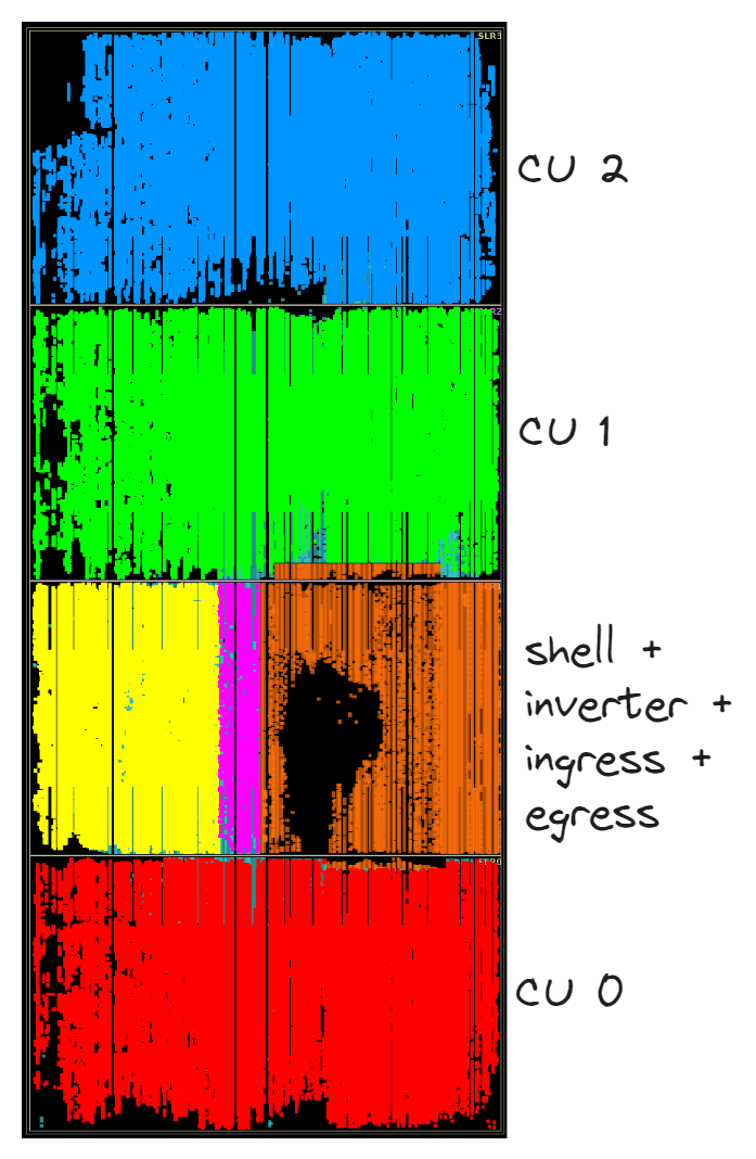
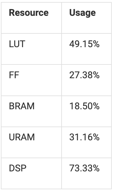
As shown in the table below, our total resource usage is quite low. This means there’s definitely room to grow! While we do not have enough DSP resources to instantiate another compute unit, we can spend our LUT and FF budget on aggressive pipelining to increase clock frequency.
Another interesting note is our power consumption is only 120W, which is split between 85W for MSM computation and 35W for the shell (this includes DDR4 and PCIe infrastructure). This means we have plenty of power headroom on the 225W card. If we increase our computation frequency we would expect the power consumption for the MSM portion to increase linearly with frequency, while the shell power consumption to stay approximately the same.
With plenty of resources and power headroom, we are confident that we can increase the frequency to 400MHz with only a small amount of work. This will boost the performance by a further 1.6x, allowing for 1200M EC-operations per second.
One aspect that held back the potential performance is the lack of HBM (High Bandwidth Memory) on the provided FPGA card. With enough bandwidth, we would be able to use much larger window sizes as is typically done on GPUs. This would greatly reduce the number of EC-operations required to compute an MSM.
Conclusion
We are very happy to present the first example of batched affine EC-addition implemented in hardware. With the presented FPGA design we are now within cannon shot range to performance that is only currently achievable on high-end GPUs.
We should keep in mind that the U250 FPGA card was released in 2018, based on the TSMC 16nm process. We are looking forward to the upcoming cards from AMD based on 7nm and 3nm, which will greatly increase performance. One particular feature we are looking forward to is the Network-on-Chip, available on AMD’s Versal devices, which would greatly simplify the complicated data movement encountered in our design.
Furthermore, our latency-tolerant design opens up interesting new avenues for exploration. Such as: using the high latency AI-Engines in AMD’s Versal devices, and combining the raw computational power of GPUs with the flexibility of FPGAs for further acceleration.
Finally this leads us to heterogeneous computing. Zero knowledge proofs are not just about MSMs, there are a myriad of operations that need to be accelerated in order to achieve end-to-end acceleration. It is important for CPUs, and accelerators to work together in an integrated, heterogeneous fashion. We are already seeing heterogeneous computers being launched by the major hardware vendors, such as Nvidia’s Grace-Hopper, AMD’s MI300A and Versal products. Onwards to end-to-end ZK-acceleration!
Check out our joint presentation with @hamid_r_salehi of AMD at ZK-Accelerate Athens!


