This is a part one of a two-part series. In the follow-up post we will introduce the NMIT (normalized Integer Multiplication Throughput) framework used for theoretical analysis in this work as well as real benchmarks based on ZScore. For Background on ZK hardware Measurements, please refer to ZK-Score.
As the computational demand for AI inference increases at the edge and in the data-center, manufacturers are integrating power-efficient AI engines into their devices. AMD’s new AI-Engine architecture, called XDNA is one such example, and are currently available in select Versal FPGAs and laptop CPUs. What’s interesting for us, in the context of ZK acceleration, is their excellent integer multiply performance.
There are currently two versions of AI-engines available from AMD; AIE, and AIE-ML. In this post, we will focus on AIE-ML, which is the most recent generation, and has better integer multiply throughput.
The XDNA architecture is essentially a 2-dimensional array of AIE processor tiles and memory tiles, interconnected by a configurable network. The memory tiles can store 512KB of data each and is analogous to a GPU’s L2 cache, except there is no automatic caching logic, all data movement is controlled by the user.
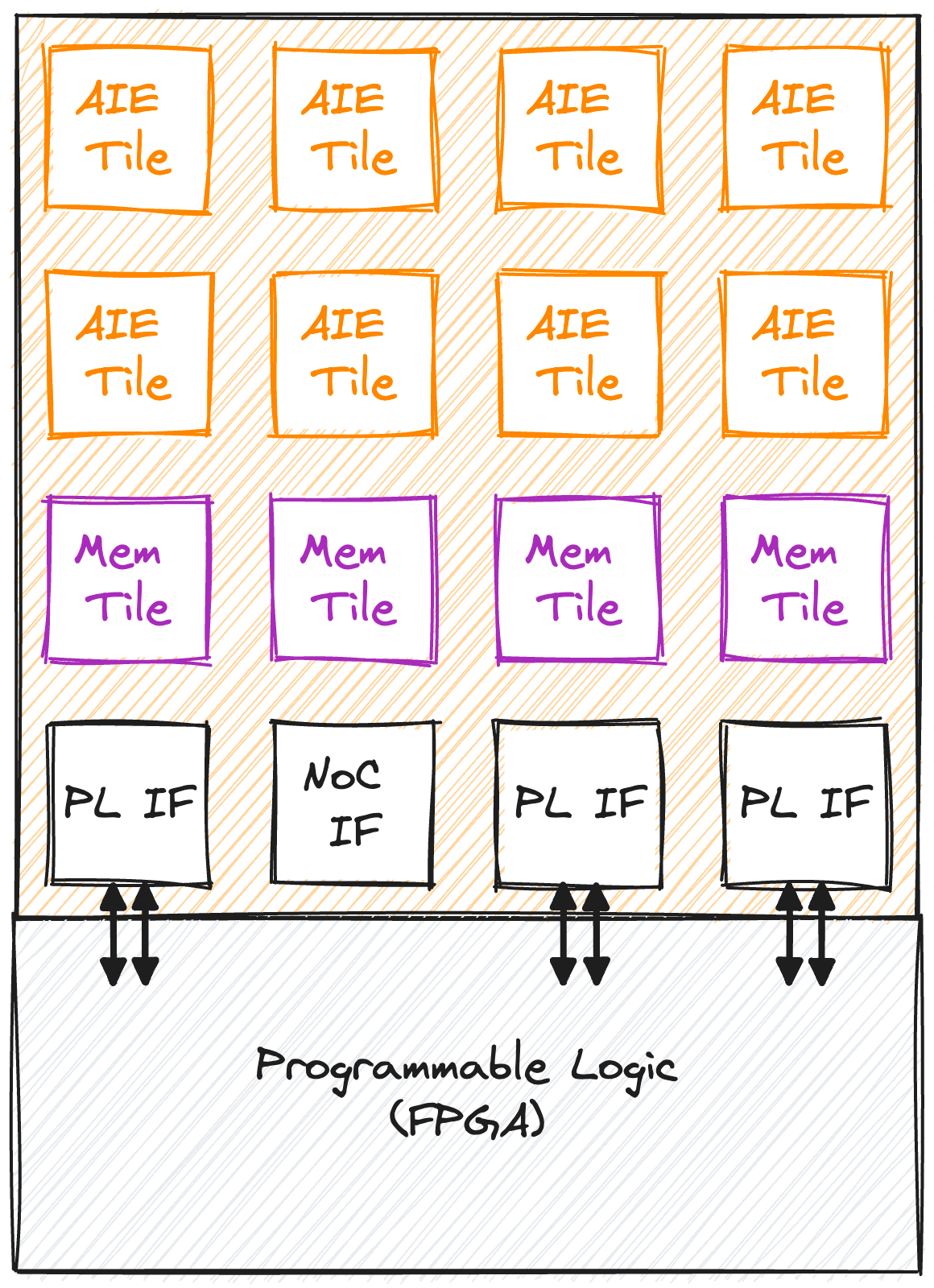
Each processor tile is capable of running an independent program and consists of a scalar unit, and a vector unit that is capable of 64 16b x 16b = 32b multiply accumulates per cycle. The hardware also allows for the emulated throughput of 16 32b x 32b = 64b multiplies per cycle.

The combination of the scalar and vector units make for a familiar programming model that is similar to vector programming on CPUs. The program for each AIE tile can be written in C++ while using intrinsics to instruct the vector unit.
At first glance this architecture seems similar to GPUs, however the main architectural difference is in its memory hierarchy. Whereas communication between cores in CPUs and GPUs are based on a strict memory/cache hierarchy, the way in which processors access memory in XDNA is much more loose and distributed.
Each processor tile can share its 64KB data-memory (not to be confused with mem-tiles) with its neighbors (shown below in blue), and is able to directly push register data into its east and south neighbors (shown in green below).

Additionally there is a packet-switched network that connects any tile to any other tile at a variable bandwidth depending on runtime congestion.

Given the memory hierarchy, one can imagine data flowing spatially through the array, like a cross between an FPGA and GPU. This kind of architecture is sometimes referred to as a Coarse-Grained-Reconfigurable-Array (CGRA).
For our analysis we will consider each AIE-ML tile as having a throughput of 16 30b x 30b = 60b per cycle. The reduction in operand width is due to the fact that the architecture does not support any carry flag, which is useful when implementing multi-precision multiplication. As such, we limit the maximum product to 60-bits which would allow for up to 16 accumulations without overflow.
Let’s compare 3 hybrid FPGA-AIE devices:
AMD Versal AI (TSMC 7nm):
- AMD VC1902 (400 AIE Tiles @1.25GHz)
- AMD VC2602 (152 AIE-ML Tiles @1.25GHz)
- AMD VC2802 (304 AIE-ML Tiles @1.25GHz)

Dethroning the Efficiency King?
Now let’s compare the AMD Alveo V70 card which is based on the VC2802 chip. The V70 seems to be directly positioned as a competitor against NVIDIA’s L4 in the datacenter AI inference space, offering basically the same form-factor, power consumption, and INT8 TOPs.

However, for ZKP which depends on big-integer performance, the V70 seems to have a distinct advantage.

When adding the V70 to our chart, we see that the V70 significantly outperforms the L4 in both throughput and taking the crown in power efficiency. Unfortunately the V70 is also power limited at 75W, reducing the achievable throughput of the VC2802 chip. However, the 75W power limit does allow for amazingly dense compute as demonstrated by Gigabyte with their G293-Z43 server, which packs up to 16x V70s in a single 2U chassis. An additional density advantage of the V70 is that it’s one of the first accelerator cards to support PCIe Gen5 speeds, and is therefore able to communicate with the host at Gen4x16 speeds while using half the number of physical PCIe lanes.
We should note that one big advantage in favor of the L4 is external memory capacity and bandwidth:
- L4: 24GB GDDR6 @300GB/s
- V70: 16GB DDR4 @76.8GB/s
External memory bandwidth can become the bottleneck in certain applications.
The Future is Heterogeneous
In this post we examined the integer throughput and efficiency of a variety of CPUs, GPUs, FPGAs, and XDNA+FPGA hybrids. We saw that XDNA augmented FPGAs currently achieve the highest big-integer multiply throughput per watt. However, raw integer multiplies do not make a full application.
Real applications, ZKP included, are complex and contain parts which are not easily offloaded onto an accelerator or are not easily parallelizable. If we throw a bunch of accelerators onto a problem we will quickly run up against Amdahl’s law. As such we need to take a full system-level view of the problem, minimize data movement, while using the right compute engines for each task. This is the promise of heterogeneous computing, and this is where the computing industry seems to be headed. Over the next year we will see big-iron datacenter GPUs with integrated CPUs, such as NVIDIA’s Grace-Hopper superchip and AMD’s MI300.
These devices allow for the CPU and GPU to share a unified memory space, eliminating the need for host-to-accelerator transfers. The future is already here with Apple’s M-series SoCs which have unified memory, allowing for zero-copy sharing of memory between the CPU and GPU cores.
Looking back at the Versal devices, including the VC2802 chip used in the Alveo V70, we also have a heterogeneous architecture. The same chip integrates CPU, FPGA, and AIE, all on a unified address space. The dual-core ARM A72 processors, while weak compared to your average x86 host, are fully capable of running Linux, networking, and yes, your Rust crates too 🦀.
On the XDNA front we already have enhanced AIE-ML engines (on TSMC 4nm) integrated into laptop SoCs. The AMD Ryzen 7040-series has up to 16 AIE-ML tiles and SoCs coming next year are rumored to have up to 64 tiles. These small AIE arrays can bring desktop-class ZKP performance while sipping a single-digit number of watts. Perhaps even more exciting is that XDNA-enhanced datacenter CPUs (Epyc) are on the AMD roadmap.
However, it is currently unknown if we will have bare-metal access to these engines like in the Versal devices.
In closing, we think that the currently available Alveo V70 is a great fit for ZKP acceleration (that’s not memory bottlenecked) and we’re looking forward to see further development with this technology.